Mario Berger, GOEPEL electronic GmbH
1 Testing in an Integrated Circuitry
Since the existence of integrated circuitries, there has been the necessity to check their functions. In the case of digital circuitries, a test is quite simple: all possible test vectors are applied in succession, and then the circuitries’ reactions at the outputs (actual value) are compared to the expected patterns (nominal value). If there are no differences the circuitry is correct.
The number of test vectors is manageable for a simple AND gate with two inputs. According to Moore and McCluskey the following formula calculates this number:
Q=2 (x+y)
Q = minimum number of test vectors
x = number of inputs
y = number of storage elements (for sequential circuits)
Because an AND gate normally doesn’t have storage elements, there are only four necessary test vectors – which is a manageable number. If this calculation is done for a circuitry with assumed 25 inputs and 50 storage elements, the problems in chip developments the engineers faced in the 1970s become obvious.
In the early 1970s, IBM gave birth to a path breaking idea: the invention of the first “Level
Sensitive Scan Design (LSSD)” method. For this purpose, existing storage elements in a chip are extended in their functions. They get four additional connectors: an input (IN), an output (OUT) and two clocks (A and B); see image 2. With these additional resources it is also possible to access the storage elements’ inputs and outputs.
In the beginning of the 1980s, the problem of “increasing complexity of the PCBs with higher packaging density” at board level was tackled. The “Joint European Test Action Group”, founded in 1985, was one of the first institutions that dealt with the topic. In those days, this group consisted of test engineers from the big European chip manufacturers. In 1986, additional North American companies joined, and the group was renamed “Joint Test Action Group (JTAG). JTAG engineered a methodology, which came close to the LSSD method developed by Ed Eichelberger. It also defines storage elements within a chip which are connected in a shift chain. The only difference was that the storage elements were additionally placed at the component’s peripheral, “at boundaries”.
For this reason, the developed method was named Boundary Scan. It was standardised as 1149.1 “Standard Test Access Port and Boundary Scan Architecture” by the “Institute of Electrical and Electronics Engineers (IEEE)” in 1990.
2 The Boundary Scan Standard IEEE1149.1
The Boundary Scan Standard IEEE1149.1 describes the static, digital interconnection test. Talking about Boundary Scan or JTAG always means IEEE Std. 1149.1. The standard determines the architecture of a Boundary Scan component, and also the description language “Boundary Scan Description Language (BSDL)”, which unveils the Boundary Scan resources unique for each component.
The IEEE Std. 1149.1 defines the inner architecture of a Boundary Scan chip, which must consist of four essential constituent parts:
– one Test Access Port (TAP)
– one TAP Controller
– one Instruction Register
– one or more data register(s)
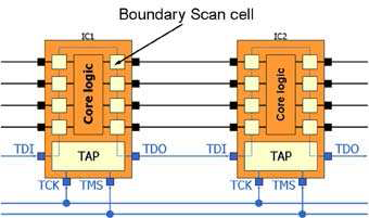
Test Access Port (TAP) The “Test Access Port” represents the interface between the Boundary Scan logic within the component and the environment. Three inputs (plus an optional fourth) and an output are described. The inputs are:
– Test Clock (TCK)
– Test Mode Select (TMS)
– Test Data Input (TDI)
– Test Reset (/TRST) optional
The output is:
– Test Data Output (TDO)
Both signals TCK and TMS as well as the optional /TRST signal are broadcast signals, whereby TDI builds a serial chain to TDO, the so called scan chain or scan path. On board level one it is called test bus. Never more than four (optionally five) signal lines are required – regardless how many components are switched in the scan chain.
Image 2: Test bus wiring of two Boundary Scan Ics
In the Boundary Scan chip, “Test Clock”, “Test Mode Select” as well as “Test Reset” are directly connected (statically) with the “TAP Controller”. The “TAP Controller’s” state is exclusively defined by these signals. That means additionally that all Boundary Scan components in a scan chain have the same TAP state. But it does not mean that all components must have the same operation mode/instruction.
TAP Controller
The “TAP Controller” is responsible for the entire control of the Boundary Scan logic in the
chip, i.e. it is responsible, among others, whether a Boundary Scan cell (see chapter
Boundary Scan Cell ) is activated or deactivated and if it is to measure or drive.
At the heart of the “TAP Controllers” there’s the “TAP state machine”. Contained states have different influences on the control of the internal Boundary Scan logic.
Instruction Register
The “Instruction register” decides on the operation mode of the Boundary Scan IC, which in turn influences the Boundary Scan cells’ control as well as the selection of the data register switched in the actual scan chain (register between TDI and TDO). The IEEE Std. 1149.1 defines three mandatory instructions:
– BYPASS
– SAMPLE/PRELOAD
– EXTEST
For each instruction there is a respective instruction code (bit code). It can be freely defined by each chip manufacturer (exception is the BYPASS instruction that must completely consist of digits 1). The length of the command register can be defined arbitrarily . An example arrangement is shown in Table 1. Thereby, the instruction register’s length was defined to two bit.
Table 1: Example for an instruction register definition
Data Register
A Boundary Scan component may contain several data registers. They’re used to file or read out information in the component. The IEEE Std. 1149.1 describes minimum two mandatory data registers:
– bypass
– boundary scan
Additional registers are possible as well, e.g. the “device identification” or colloquially called “idcode” register. The “bypass” register is the opportunity to liberate a component from an interconnection of Boundary Scan ICs, or to “bypass”. Its minimal length is just one bit. The bit’s value is unchangeable and defined with 0. The “boundary scan” register, which expresses the succession of the single Boundary Scan cells, is much more interesting for later testing. Because each chip has a different number of Boundary Scan cells, the register length is variable.
Boundary Scan Cell
The Boundary Scan cell is the essential element of the Boundary Scan Test methodology. All described constructs’ functions are only for the correct control of the respective Boundary Scan cells.
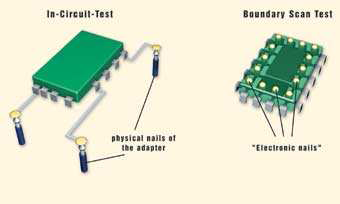
The Boundary Scan cell is the ingenious opportunity to control a component pin disengaged (?) from its normal functionality, i.e. to drive or measure a particular level. For this purpose, the Boundary Scan cell is situated between the component’s core logic and peripheral (output driver, input driver). Because of the functionality similar to the physical contact nails of the In Circuit test technology, which implement access to the test points on a board, the Boundary Scan cells are also called “electronic nails”.
Image 3: Comparison of the test methods ICT and Boundary Scan
A Boundary Scan cell’s internal architecture can be highly different. In its version from 2001, the IEEE Std. 1149.1 describes ten different cell types (BC_1 to BC_10). The cell may have individual structures, whereby the arrangements are very often very similar.
Boundary Scan Description Language (BSDL)
Each Boundary Scan component has a specific Boundary Scan structure, this is decisive for test engineers or test software to work usefully with such a component. IEEE Std. 1149.1 mandatorily dictates core requirements, but leaves scope for individual developments. This is necessary – as will be seen for the example of structure/number of Boundary Scan cells: an IC with 20 pins has a lower number of cells compared to an IC with 1,500 pins. The “Boundary Scan Description Language (BSDL)” was developed to describe this individuality. It is the exchange platform between chip manufacturer (only they can can know the interior of their chips) and test engineer (who wants to use the interior of their chips). The BSDL file is a data that provides specifications about:
– available test bus signals (particularly information about the existence of an optional /TRST signal and maximum TCK frequency, up to which the component can be operated)
– possible “compliance” pins
– instruction register (available instructions incl. bit code; instruction register length)
– data register (available data register incl. Possible predefined values, e.g. IDCODE of the chip)
– Boundary Scan cell structure (number, type, function, assignment to IC pin)
3 Possibilities and Limitations of IEEE Std. 1149.1
The static, digital interconnection test compliant with IEEE Std. 1149.1 enables everything
that is situated in the digital area and is not time critical. Thus, it is possible to test resistors (for presence), crystals, driver ICs, logic gates, reset ICs and even RAM ICs or Flash ICs (parallel as well as serial). For example, for the latter the necessary write and read protocols are simply imitated via the Boundary Scan component pins. This is the same functionality as a functional test, but slower because of the serial Boundary Scan chain. And that’s the test methodology’s limitation: the maximum possible switch/measuring frequency at the IC pins. It is the result of the number of Boundary Scan cells (therefore the “boundary scan” register length) and the “Test Clock” frequency. It doesn’t matter whether the signal level of one or several component pins should be changed – in each case it must be shifted through ALL cells.
The shift process in a medium sized Boundary Scan component with 500 Boundary Scan cells and a typical frequency of 10 MHz takes 50 s. However, one shift process can initiate a single signal change at the IC pin. For the opposite edge another shift process is required
which results in a maximum achievable frequency of 100 s1, hence 10 kHz.
4 What advantages do modern tools bring?
Due to contemporary knowledge, there are some basic requirements to a Boundary Scan
test system. The user doesn’t want to bother the correct switching of the “Test Mode Select”signal to access the right graph in the “TAP state machine”. Furthermore, he doesn’t want to bother with a “TAP state machine”. At most, he wants to define the operation modes for the Boundary Scan ICs. Fortunately, modern tools effectively relieve this tiresome labour.
What does the term Boundary Scan tool generally mean?
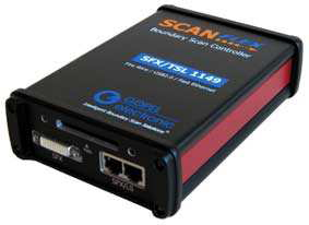
A Boundary Scan test system consists of hardware and software. The hardware has “only” to be able to control the TAP signals. Each Boundary Scan hardware worldwide features this basic functionality (but there are partly important differences in performance, real throughput and flexibility).
Image 4: Hardware – Boundary Scan Controller from GOEPEL electronic (SFX TSL1149.x) Boundary Scan vendors differentiate in the software, and that’s why usually software is meant when talking about Boundary Scan tools. Modern Boundary Scan Software is expected to automatically generate necessary test vectors and probably lead the operator quickly to the fault area on a test object, i.e. a best possible diagnostic. If the integration of Boundary Scan test in a production line or other test system is considered, there’s the demand that a modern Boundary Scan tool must provide respective interfaces.
5 Design for Testability (DFT)
The best Boundary Scan test systems with the most powerful Automatic Test Program Generators (ATPG) are helpless if particular design rules were not observed during schematic design or even a step earlier during component selection. The following criteria show a narrow selection of the arguably most important “design for testability” rules: Compliance Pattern Using Boundary Scan components, it is common to share the TAP pins with other functions, e.g. debugging. For that reason, such a component usually has a pin that determines the function. Such a pin could be named e.g. JTAG#/DEBUG, and would activate the debug mode with a high. In this example, a low must be applied at the pin, so that it can be tested with Boundary Scan.
Test Bus Termination
A good test bus termination is essential for a fast test execution. As guiding principle, test
time is proportional to the “Test Clock” frequency.
Modern test systems are able to process the TCK signal with 80 or even 100 MHz. It’s critical to take reasonable care during TAP signal wiring.
Image 5: Test bus termination
Flexible Scan Chain
It is common practice to produce boards in different assembly variants. Caution is advised if such an assembly variant is on the Boundary Scan components. It may happen that an IC is missing in the scan chain, i.e. the serial path (TDI TDO) is broken. The result would be a complete failure.
5.1 Access = Success
“Access = Success”; this “Design For Testability” key rule is valid for the Boundary Scan test technology as well as the classic In Circuit test method. Only the implementation is different in both cases. Applying the In Circuit Test means to set test points where possible. On the contrary, in the case of Boundary Scan they are “sleeping” partly unused in the Boundary Scan components in terms of unwired IC pins. Normally, these are pins (especially in terms of programmable logic chips) not required during the “normal” function of a PCB. Two typical examples are to show how the unused “test points” can be applied to significantly increase test coverage.
Image 6: RAM bank with PLL
As the first example, image 6 shows a RAM bank whose clock is distributed by a PLL. But a
static access to all IC pins is required to test the RAM components with Boundary Scan. This is not given for the clock signal by the PLL, which leads to a higher loss in test coverage.
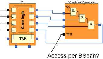
Image 7: …
Image 7 also shows how decisive access to a single IC pin is for the testability of a complete
component. The image shows a component with integrated NAND tree test. It could
optimally be tested per Boundary Scan, provided that the NAND tree test must be activated with a specific signal level at a predetermined IC pin (in image 7 it is named “TEST”).
6 Future Standards
The success of the JTAG/ Boundary Scan standard IEEE1149.1 has inspired and encouraged all participants to improve the test technology, making it more boundless. Two out of numerous newly developed ad partly passed standards are shortly introduced in this chapter.
IEEE1149.4
The breakthrough of standard IEEE1149.4 would possibly mean the end of the classic In Circuit Test, because it is a “mixed signal” or also analogue interconnection test.
The method is very simple. In addition to the four (optionally five) TAP signals two “Analogue Test Access Port (ATAP)” signals “Analogue Test 1 (AT1)” and “Analogue Test 2 (AT2)” are required. These additional pins can be internally switched independent from each other per test bus instruction to any pin of a component that is IEEE Std. 1149.4 compliant. One might say that an IEEE1149.4 component has an internal relay matrix, which can be switched to any pin via test bus. If the ATAP is connected with some external methodology, a classical In Circuit tester is built (with limited functions).
IEEE1149.6
The standard IEEE1149.6 enables testing of serial, digital high speed connections. It describes the “Advanced Digital Network” interconnection test. To work with the existing TAP signals is its biggest advantage. The standard requires a few extra instructions, a slightly extended Boundary Scan cell and an integrated test pattern generator. The principle again is very simple. Some pins of the IEEE Std. 1149.6 compliant IC are connected to a new type of Boundary Scan cell. In contrast to the “old” cell types, this new cell has a special input, which is connected to the internal test pattern generator. Per instruction, the Boundary Scan cell switches to the new input and the test pattern generator sends the test pattern to the Boundary Scan cell, thus to the component pin, independently from the “Test Clock” signal. This applies for sending. At the same time on the receiver side, the test pattern is read in and written in a buffer.
Afterwards, the test pattern from the sender is compared und a Pass/Fail statement is made. This statement is filed in a Boundary Scan cell as 0 or 1, and can be read out and evaluated by the test system.
7 Summary
JTAG/ Boundary Scan is the most ingenious test technology. It is the jump from physical access to a board’s conductor tracks (necessary for the In Circuit Test) with all its physical limitations to an electric and, therewith, unlimited access. JTAG/Boundary Scan only requires four control lines and only a fistful of important “Design for Testability” rules.
Talking about JTAG or Boundary Scan, one refers to the IEEE Std. 1149.1 – thus the static, digital interconnection test. Its limitations are to be found in the analogue area as well as
high speed area. But brand new approaches and solutions referring to the standards IEEE 1149.4 and 11149.6 have extended the utilisation of JTAG/Boundary Scan in these areas. A Boundary Scan test developer doesn’t have to deal with each and every detail of the technology since modern tools, based on component models, execute the greater part of his tasks.
