My name is Kathleen Yu, and I am an incoming junior studying Electrical Engineering at Arizona State University. This past summer, I was given the opportunity to be a Summer 2026 PCB Design Intern for MJS Designs. My experience working here was truly insightful and amazing. I was able to learn a lot about everything that goes into manufacturing printed circuit boards.
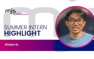
During the first two weeks of my internship, we toured all the different sectors of the company, which allowed us to see each step in the PCB production process. On these tours, we got to see all kinds of cool equipment in action that I hadn’t got the chance to see in person before. I was able to watch a flying probe machine test boards, check out the soldering operation stations, and see the surface mount technology assembly line running up close. Every other week, I would alternate between the Engineering and Design departments with a fellow intern, Khiem. This schedule allowed us to learn valuable and distinct skills under two seasoned mentors.
When I was in the Engineering office, I learned how to create schematic captures, model board fixtures, program microcontrollers, and configure the underlying logic behind schematics. As for my time in the Design section, I was introduced to new CAD software, footprint design, datasheet analysis, and BOM generation. The people I worked alongside were what also made my internship a pleasant and informative experience. The company’s Director of Engineering, Devin DeGarmo, oversaw my work and training whenever I was stationed in the Engineering department. I also trained under another Electrical Engineer, Adrian So, during my time in Engineering. With their knowledge and involvement in many high-stakes projects, I refined my ability to carefully assess and manage schematic captures, as well as to find the best-suited components for the board. A lot of the work was foreign to me, but their guidance and mentorship made all of it easier.
When I worked in the Design department, the Senior Design Manager, Albert Castro, helped me understand PCB layouts and footprint creation, and gave me a glimpse into routing/tracing boards. His 25+ years of experience and proficiency in designing even the most complex boards made him a great instructor and supervisor.
We also got to experience a new side of the business when us as interns tagged along with Neil, the Director of Business Development, to the ASU SkySong 2026 E-Mobility and Clean Energy Summit. We helped set up the MJS booth for the conference there, which was great because it gave us a chance to witness firsthand how a company presents itself and interacts with potential customers in the professional world.
What I appreciated was that I could tell that the internship was meant to ensure that we learned a lot. Some of my favorite moments from the engineering side were just brainstorming by the whiteboard, thinking about different approaches to problems, and sketching out the math and logic. I also loved getting the chance to work with VHDL to code the DE10-Lite FPGA board and the MJS Flying Probe Board. My most memorable moments in the Design room consisted of learning about what exactly makes up a PCB and getting industry-expert advice from Albert. I was given the time needed to expand my theoretical knowledge to new horizons. There were days when a schematic or circuit design wouldn’t cooperate on the first try or work exactly as I had imagined it to, but I further understood that’s what patience, guidance, and the massive reach of internet resources are for.
Over those three months, I picked up so much. I acquired knowledge that I would not have been able to learn as easily on my own or through a company that did not prioritize quality as much as MJS Designs does. From writing code and putting programs to the test to getting deep-dive explanations on how every tiny component and region of a board is assembled together, I was given all the materials I needed to grow. It even gave me a head start in some of my classes for the Fall semester because of everything I learned on the job. I gained a deeper appreciation for hardware engineering and PCB production now that I see how much effort and thought goes into making these premium boards.
Looking back, my time at MJS Designs was invaluable. My attention to detail and my inspection skills have improved, and I finally got to see how a real, engineering-focused workplace runs. I am grateful for this experience and want to give a big thank you to everyone at MJS for making it a special one. I’ll remember this as the kickstart to my career as an engineer and my life’s dream.