
Stack-up modeling and development is an essential step in the printed circuit board (PCB) design process. It involves determining the ideal layer arrangement, material selection, and the thickness of each layer that will make up the PCB. Stack-up modeling is critical for several reasons, two of which are the electrical performance and for the manufacturing considerations.
Electrical Performance In A Stack-Up
PCB stack-up modeling is crucial for ensuring optimal electrical performance of the circuit board. The arrangement of the different layers of a PCB can greatly affect its electrical properties, such as signal integrity, power distribution, and electromagnetic compatibility (EMC).
Signal Integrity
One of the main goals of PCB stack-up modeling is to maintain signal integrity, which refers to the ability of a signal to maintain its original form and quality as it travels through the PCB. The material selection, arrangement of signal layers, ground planes, and power planes in a stack-up should be carefully considered. The location of the signal layers is preferred to be placed adjacent to a ground plane in order to control the characteristic impedance of transmission lines on a PCB and provide shielding from external and internal electromagnetic interference (EMI). Maintaining a consistent characteristic impedance throughout the board can reduce signal reflections and ensure reliable signal transmission.
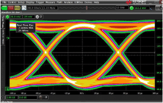
Eye Diagram For Signal Integrity Evaluation Of High-Speed Data Quality.
Power Distribution
PCB stack-up modeling is also important for ensuring proper power distribution on the board. The placement of the power planes can affect the power delivery network (PDN) of the board, which determines how power is distributed to the different components and circuits. A well-designed PDN can minimize voltage drop, provide a stable voltage reference, has greater current carrying capacity, improves heat dissipation, has a short return path, and provides better decoupling. A ground plane provides a low-impedance return for voltages and signals, reduces EMI, and minimizes noise.
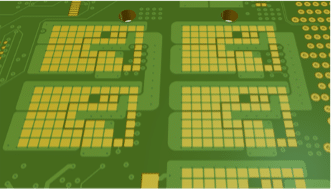
Power Supply Layout Using LGA footprints.
Electromagnetic Compatibility (EMC)
EMC refers to the ability of a device or system to operate properly in the presence of EMI. EMI can be generated by both internal and external sources, such as nearby circuits, cables, and wireless devices. A well-designed stack-up can provide shielding and isolation between different components and circuits, reducing the coupling of the electromagnetic fields, and is important in reducing EMI by minimizing the loop area of the circuits. The use of ground planes provides a low impedance signal return paths that reduce the emission of electromagnetic radiation from the board.
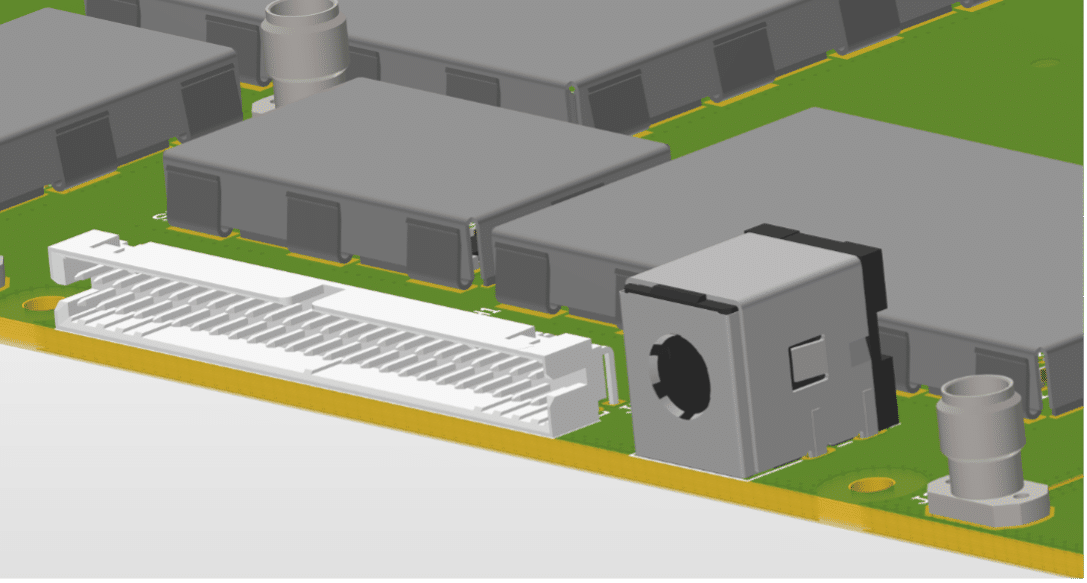
Image Of EMI Sensitive Assembly
Manufacturing Considerations For A Stack-Up
The PCB manufacturing process also influences the stack-up development. Stack-up modeling takes into account the available technology and helps to ensure that the board can be manufactured efficiently and cost-effectively. The following are some important manufacturing considerations to keep in mind when modeling a PCB stack-up.
Layer Symmetry
A symmetrical stack-up, where the copper layers and dielectric layers are balanced around the center of the board, is easier to manufacture and can reduce warpage and distortion during the lamination process.
Material Selection
The metal and dielectric materials should be compatible with the manufacturing process, desired electrical performance, and must be able to withstand the thermal and mechanical stresses during production. Solder mask should also be taken into account in the stack-up modeling, especially for RF and high-speed designs because it is considered a dielectric material.
Copper Weights And Traces
The copper weight and trace width on the PCB must be optimized for the manufacturing process. Heavier copper weights and narrower traces can be more difficult to manufacture.
Aspect Ratios Of Vias And Holes
The aspect ratio of a hole in a printed circuit board (PCB) is the ratio of the PCB thickness to the diameter of the drilled hole. For manufacturing, aspect ratio should be kept as low as possible for the plating process and for drilling.
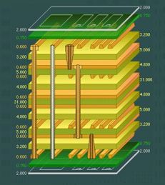
Stack-Up Model
Overall, the success of a PCB design greatly depends on the careful consideration of both electrical and manufacturing considerations during the stack-up modeling and development process. A well-designed stack-up can result in a PCB that is both electrically reliable and manufacturable, providing long-term performance and durability for a wide range of applications.
MJS Designs has more than four decades of experience in providing top-quality PCB design services, and is highly regarded for its commitment to delivering innovative and reliable solutions to its clients. Our design team remains up-to-date with the latest industry standards by attending various conferences, workshops, and classes, ensuring that their clients benefit from the most cutting-edge PCB layout solutions available. If you’re interested in learning more about how MJS Designs can help bring your project to fruition, click here.