
The minimum trace width and spacing for copper on a printed circuit board (PCB) are critical design parameters that significantly impact the overall performance and reliability of the board. These parameters directly affect the manufacturability, design density, signal integrity, electrical characteristics, environmental considerations, and overall functionality of the PCB. The successful use of acceptable trace widths and spacing greatly depends on careful consideration by MJS Designs’ PCB designers, then the PCB design must be validated and verified by one of our in house DFM CAD Specialists (design for manufacturing) utilizing Valor NPI for a full DFM Analysis.
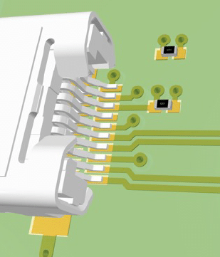
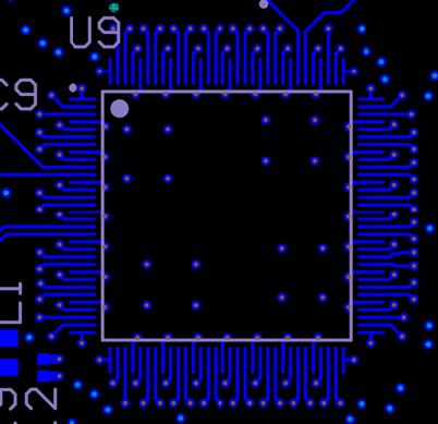
A trace is a thin copper conductor that connects various components, such as integrated circuits (ICs), resistors, capacitors, and other electronic devices on a PCB. It serves as a pathway for the flow of electrical current and the transmission of signals between these components. The trace width is the dimension of the copper conductor in the horizontal plane, typically measured in mils or millimeters. The trace spacing, on the other hand, refers to the distance between adjacent traces, also typically measured in mils or millimeters.
MJS Designs will delve into the importance of minimum trace width and spacing for copper in PCB design and explore the various factors that influence these parameters.
Manufacturability
PCB manufacturing processes, such as etching and plating, are directly affected by the minimum trace width and spacing. These parameters impact the accuracy and reliability of the fabrication process. If the traces are too narrow or too closely spaced, it becomes challenging for manufacturers to etch and plate the copper pattern accurately, leading to potential shorts, opens in the traces or unacceptable trace width and spacing. Adhering to appropriate trace width and spacing guidelines, MJS Designs ensures manufacturability and avoids potential manufacturing defects. The capabilities of the PCB manufacturer and the fabrication processes employed play a significant role in defining the minimum trace width and spacing. Different manufacturers may have different equipment and processes, leading to variations in their manufacturing tolerances and capabilities. MJS designers considers these capabilities while setting the minimum trace width and spacing to ensure the design can be reliably manufactured.
Design Density
The overall density of the PCB design influences the available space for traces. MJS designers must balance the density with the practical limitations imposed by the number of components, pitches of devices, layer count, manufacturing processes, electrical, thermal, and mechanical constraints. Higher design density may limit the trace width and spacing options, requiring careful optimization to achieve the desired functionality and manufacturability.

Signal Integrity
The minimum trace width and spacing directly impacts signal integrity by influencing impedance control, signal propagation, and the prevention of signal degradation. MJS designers must consider the design density when determining the minimum trace width and spacing to meet the signal integrity requirements. Higher design density often corresponds to more complex and sensitive circuitry, including high-speed digital or analog signals. Maintaining signal integrity is crucial in such designs to ensure reliable data transmission. Experienced designers at MJS Designs are responsible for managing and maintaining the rules within the PCB design software in order to control the trace widths and spacing to meet the signal integrity requirements.
Electrical Characteristics
The electrical characteristics of a PCB, such as impedance, capacitance, and resistance, are directly influenced by the trace width and spacing. These parameters play a vital role in determining the impedance matching and signal integrity of high-speed digital and analog circuits. A trace with inadequate width can increase resistance and impedance, leading to signal degradation, crosstalk, and reflections. Additionally, improper spacing between traces can cause capacitive coupling, leading to unwanted signal interference and reduced performance. Therefore, maintaining appropriate trace width and spacing is essential for maintaining the desired electrical characteristics of the PCB.
Current Carrying Capacity
The amount of current a trace is expected to carry affects its required width. Higher current necessitates wider traces to minimize resistive losses and prevent overheating. Copper traces on a PCB can carry significant amounts of electrical current, particularly in power circuits and areas with high-power components. MJS designers considers the current-carrying capacity of the traces and calculates the sufficient width accordingly. Trace width affects the resistance of the conductor, and a narrower trace width leads to higher resistance. Increased resistance results in higher power dissipation and elevated temperatures, potentially causing thermal issues and affecting the overall reliability of the board. By ensuring an adequate trace width, designers can minimize resistive losses and facilitate effective heat dissipation, preventing overheating and potential component failures.
Voltage Drop and Power Distribution
In power distribution circuits, where high current flows through the traces, the trace width becomes crucial in minimizing voltage drop. A narrower trace leads to higher resistance, resulting in an increased voltage drop across the trace. This can negatively impact the power distribution and cause voltage fluctuations, affecting the performance of the connected components. MJS designers maintain an appropriate trace width to minimize voltage drop, ensure efficient power distribution, and prevent other voltage-related issues.

Environmental Considerations
PCBs are often subjected to harsh environments, including temperature variations, humidity, and exposure to chemicals. The trace width and spacing influence the robustness and reliability of the board under such conditions. MJS designers considers the various conditions to provide adequate trace width and spacing to help ensure the PCB’s resilience to environmental factors and enhance its overall reliability and longevity.
In conclusion, the minimum trace width and spacing for copper on a PCB are critical parameters that impact the manufacturability, design density, signal integrity, electrical characteristics, environmental considerations, and overall reliability of the board. MJS Designs has years of experience, training, and certifications that guide our designers to develop trace widths and spacing while carefully considering these parameters to ensure optimal performance and functionality. Because trace widths and spacing capabilities and technology can change fast in this industry, MJS designers remain up-to-date with the latest industry technology and standards. In addition, the MJS Design team utilizes Valor NPI software and our own knowledgeable DFM CAD Specialist. Click here to learn more about the PCB layout and DFM analysis services MJS Designs offers to ensure a robust design.